AIF User Spotlight

Huimin Qiao is currently a postdoctoral research scholar in Nina Balke’s Group within the Department of Materials Science and Engineering at NC State University. Her primary research focuses on nanoscale characterization using atomic force microscopy, particularly exploring the multi-physical fields coupling in ferroelectric and piezoelectric materials, along with their degradation mechanisms. She’s passionate about advancing her career in the field of ferroelectrics and atomic force microscopy. She enjoys hiking, traveling, photography, cooking, gardening, and spending quality time with her cat, Bear.
What instruments are you using for your research?
Lately, I have been extensively utilizing the Helio 5 Hydra DualBeam – Plasma Focus Ion Beam for microscale cutting tasks. Additionally, I am proficient in operating the Bruker Hysitron TI980 for nanoindentation, the Zeiss XRM Nano CT for 3D imaging, Keyence instruments for height profile characterization, as well as Raman Confocal and ToF-SIMS for chemical imaging. I am also experienced in utilizing SEM and EDS for imaging cross-sections and determining chemical compositions of samples. My approach involves employing a range of instruments to gain comprehensive insights into my samples from various perspectives.
How is your research impacting the community?
I utilize atomic force microscopy to investigate the physical properties of piezoelectric, ferroelectric, and dielectric materials, focusing on their local-scale coupling. Piezoelectricity, an electromechanical effect where mechanical force generates charges and vice versa, is crucial in electronic devices as transducers, actuators, and sensors. However, cyclic electric fields can degrade ferroelectric performance, impacting device endurance and reliability. Understanding the degradation mechanism in ferroelectrics is a pivotal challenge, exacerbated by the miniaturization of electronic devices.
In my research, I employ atomic force microscopy, specifically piezoresponse force microscopy, to examine static and dynamic piezoelectric properties at nano scales.

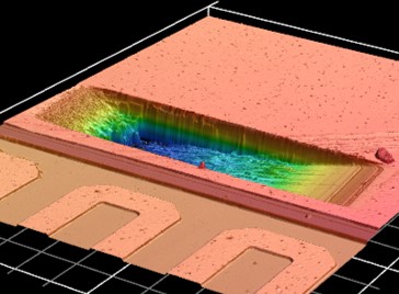
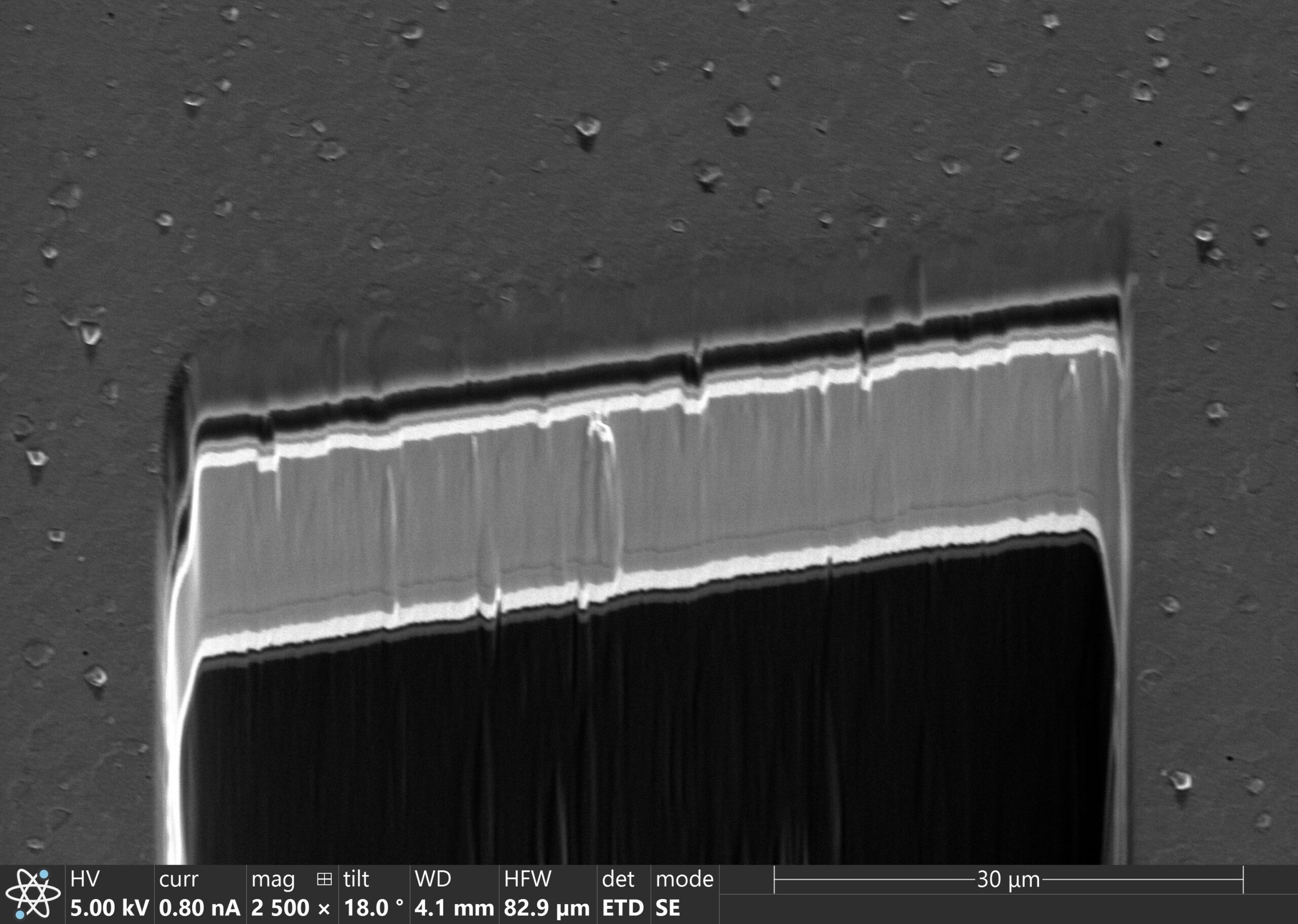
I utilize pFIB to create wedge-shaped structures in ferroelectric materials embedded in commercial chips, with Keyence used for viewing shape and height profiles. SEM and EDS provide insights into chip layering and elemental distribution relevant to ferroelectric properties, while nano CT identifies micro cracks and defects. Our aim is to elucidate degradation mechanisms across various ferroelectric materials from local to macroscopic scales.

Our objective is to understand the mechanisms governing transitions between these polar states and to manipulate them for future nanodevice applications.
– Huimin Qiao
Additionally, I investigate phase transitions in 2D ferroelectric materials. These materials exhibit robust ferroelectricity at single-layer thickness, making them promising for electronic nanodevices. Transition metal thio phosphates (TMTPs) are particularly intriguing due to their negative piezoelectricity and multiple polar states (high polarization, low polarization, antiferroelectric).
What have you learned from your experience at AIF?
Understanding the workings of an instrument is more crucial than mere operational knowledge.
Best thing about AIF in 5 words or less?
Great facilities and knowledgeable staff.
Is there a staff member at AIF that has helped you?
I am grateful to the AIF staff for their kindness, helpfulness, knowledge, and support. I would like to specifically thank Roberto Garcia for his valuable help. I also appreciate Toby Tung, Ruksana Baby, Elaine Zhou, and Chuck Mooney for their assistance in training and answering my questions.
- Categories: